 Photo credit Thor BalkhedGallium Oxide and related materials
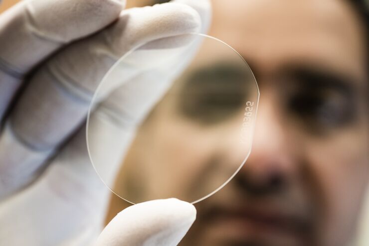
The aim is to develop of a new wide band gap semiconductor material – β-Ga2O3 for applications in high-power electronic devices with substantial efficiency gain in e.g., generation and transmission of electric power, electrification of vehicles and motor drivers. β-Ga2O3 has superior material properties such as higher band gap and break-down voltage, combined with significantly lower substrate price compared to widely studied wide band gap materials such as SiC and GaN. Initially we will primarily focus on the development of metalorganic vapor phase epitaxy of β-Ga2O3 exploring growth conditions and different precursors. This activity also includes modification of an existing growth reactor and modeling of temperature and gas flow profiles in order to optimize reactor design and growth. In parallel I will also investigate the free-charge carrier properties of β-Ga2O3 substrates and device structures grown by molecular beam epitaxy from Tamura Co. and Tokyo University. The knowledge gained in these initial studies will be used to optimize doping in our MOVPE β-Ga2O3 during later stage of developments. In this period the free-charge carrier properties will be studied as a function of doping and surface orientations. First test device structures will be designed and grown.Vertical and horizontal power devices will be fabricated and characterized in collaboration with Chalmers University.
Research financed by Swedish Energy Agency and VR
Cooperation with SweGaN, Epiluvac and Chalmers University