 Photo credit Thor BalkhedDescription of Lab
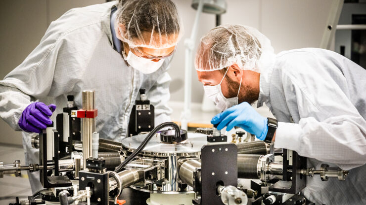
Our cleanroom consists of several different areas in ISO class 6 and 7 (FED STD class 1000 and 10 000) meaning they are built to assure less particles in the lab environment. Expert technicians and tool responsible persons are present within the laboratories, trained in a wide variety of processes and techniques. We have specific areas for lithography, evaporation, sputtering, plasma etching, electrochemistry, scanning electron and atomic force microscopy, and electrical/optical characterization. We also have a rubber lab for soft electronics and gloveboxes for performing experiments under nitrogen atmosphere. Our cleanroom facilities provide the possibility to develop, pattern, and characterize advanced soft functional materials and electronic devices of the future.
Coating and Microfabrication
High vacuum thermal evaporators are available for the deposition of common metals (Al, Ag, Au, Ti, Cr). Metal patterns with resolution down to ~50 µm are achieved with plastic shadow masks made via laser patterning or using a flat-bed cutter. Standard photolithography facilities are available to achieve smaller features of ~1 µm using etching or lift-off techniques.
Soft patterning
Plasma enhanced CVD is available to coat insulating layers and the three “Reactive Ion Etching” setups are used to pattern polymeric materials.
Synthesis and coatings
Chemical synthesis and ink formulations are carried out inside state-of-the-art fume hoods and nitrogen gloveboxes. Homogenizers, ultrasonic bath sonicators, and high-power probe sonicators are available to attain homogeneous dispersions. The resulting mixtures are deposited in a variety of manners i.e. atomically thin coatings are achieved with two “Langmuir-Blodgett” coaters, programmable spin coaters are used for tens-hundreds of nm coatings, blade coating for µm thick coatings, while electrospinning and freeze-dryers are available to attain free-standing bulks.
Material characterization
Surface morphology studies are carried out with optical microscopes, optical & surface profilometers, atomic forces microscopes (AFM), and a scanning electron microscope (SEM). Energy-dispersive X-ray spectroscopy (EDX) capability is available within our SEM system, providing the possibility to assess chemical composition of samples. UV-Vis-NIR, FTIR and ATR are available for absorption studies while dielectric properties are studied with a dielectric spectrometer for films and liquids.
Climate and Humidity chambers are used for studying materials at temperatures above 0 ⁰C and from dry to wet conditions. Low-temperature vacuum measurements are carried out inside four and six arm cryogenic probe stations with temperature ranges of 10-500K. Complete Thermoelectric (TE) characterization facilities have been developed in-house for thin films and bulk (solid and liquid) materials.
Device characterization
Two state-of-the-art Keithley 4200 systems with probe stations are used for diodes, transistors, and complementary circuit analysis. Electrochemical characterization of materials and devices (supercapacitors and batteries) are performed by potentiostats from Gamry and Bio-Logic.
Key features
- ISO 6 and ISO 7 cleanroom facility for micro-fabrication and characterization
- Develop, pattern, and characterize advanced soft, functional materials and electronic components
- Equipment for dry etching and lithography
- Several deposition-tools including thin film deposition
- Equipment for electrochemical characterization and measurements
- Precision characterization methods such as SEM and AFM
- A rubber lab to fabricate and characterize soft functional materials
- Fabrication and analysis of structures on the micron- and nano-scale
- Fully automated thermoelectric setups for lateral and vertical device characterization
- Four and six arms cryogenic probe stations for low and high temperature studies
- Nitrogen glove boxes for metal deposition/synthesis/coatings/characterization